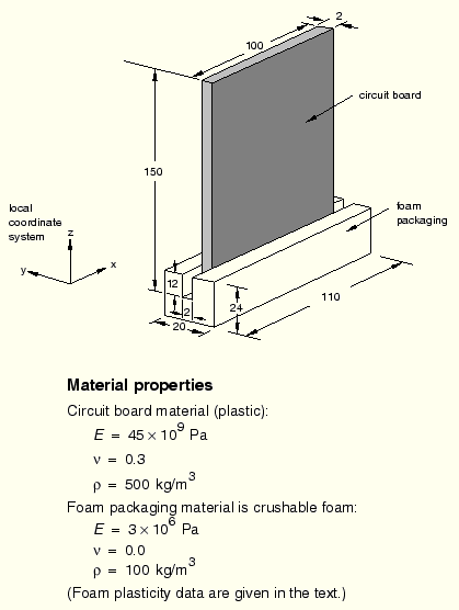
In this example you will investigate the behavior of a circuit board in protective crushable foam packaging dropped at an angle onto a rigid surface. Your goal is to assess whether the foam packaging is adequate to prevent circuit board damage when the board is dropped from a height of 1 meter. You will use the general contact capability to model the interactions between the different components. Figure 6–32 shows the dimensions of the circuit board and foam packaging in millimeters and the material properties.
While the circuit board will be dropped at an angle, it is easiest to use the *SYSTEM option to define the mesh aligned with a local rectangular coordinate system, as shown in Figure 6–32. The *SYSTEM option transforms nodal coordinates from the local coordinate system to the global coordinate system. This option allows you to define the circuit board in the x–z plane of the local coordinate system, which is rotated by the desired angle relative to the global coordinate system.
The *SYSTEM option defines a new coordinate system by specifying three points: a local origin, a point on the local x-axis, and a point in the local x–y plane. Before defining the nodes for the circuit board, use the following option to tilt the mesh so that it lands on its corner:
*SYSTEM
0., 0., 0., .5, .707, .25
-.5, .707, -.5
All subsequent nodal definitions will be in this local coordinate system. To reset the coordinate system to the default, use another *SYSTEM option with no data lines.
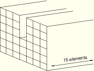
The overall mesh for this problem is shown in Figure 6–33.
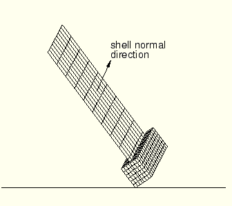
Define the circuit board so that the shell normals are in the direction indicated. Defining the bottom corner of the foam packaging as the origin of your model will ensure the correct positioning of the circuit board and packaging. Since the ground onto which the board will be dropped is effectively rigid, use a single R3D4 element for this part of the model. The packaging is a three-dimensional solid structure that should be modeled using C3D8R elements. The circuit board itself can be considered as a thin, flat plate with various chips attached to it. Therefore, model the circuit board with S4R elements, and model the chips with MASS elements.Since you will be using shell elements for the circuit board, ABAQUS/Explicit will, by default, use the original shell element thickness when checking for contact. The circuit board and its slot in the foam packaging are both the same thickness (2 mm) so that there is a snug fit between the two bodies. In this example the circuit board is a mesh of 10 × 10 S4R elements, and the foam packaging is a mesh of 6 × 7 × 15 elements, as shown in Figure 6–34.
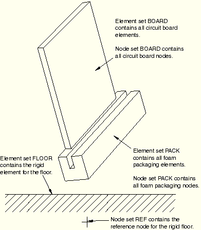
The MASS elements are positioned as shown in Figure 6–35. The mesh for the packaging is too coarse near the impacting corner to provide highly accurate results. However, the mesh is adequate for a low-cost preliminary study.Figure 6–35 and Figure 6–36 show all of the sets necessary to apply the element properties, loads, initial conditions, and boundary conditions, as well as to request output for postprocessing.
Include the circuit board elements in an element set called BOARD, and include the corresponding circuit board nodes in a node set called BOARD. Similarly, for the foam packaging include the elements in an element set called PACK, and include the nodes in a node set called PACK. The element sets will be used to refer to material properties, and the node sets will be used to apply initial conditions. Create an element set called FLOOR containing the floor's rigid element and a node set called REF containing the reference node for the rigid surface modeling the floor. Include the mass elements modeling the chips in an element set called CHIPS.Two methods could be used to simulate the circuit board being dropped from a height of 1 meter. You could model the circuit board and foam at a height of 1 meter above the rigid surface and allow ABAQUS/Explicit to calculate the motion under the influence of gravity; however, this method is clearly impractical because of the large number of increments required to complete the “free-fall” part of the simulation. The most efficient method is to model the circuit board and packaging in an initial position very close to the surface with an initial velocity to simulate the 1 meter drop (4.439 m/s).
We now review the model data required for this simulation, including the model description, the node and element definitions, element and material properties, boundary and initial conditions, and surface definitions.
Model description
Using the *HEADING option, provide a suitable heading for your model, such as the one shown below. You should use SI units in your model.
*HEADING
Circuit board drop test
1.0 meter drop
SI units (kg, m, s, N)
Nodal coordinates and element connectivity
Use your preprocessor to generate the mesh in the local coordinate system. Precede the nodal definitions with the *SYSTEM option to transform the nodes into the tilted coordinate system, as described previously. Your nodal definitions for the foam packaging and circuit board will look something like the following:
*SYSTEM
0., 0., 0., .5, .707, .25
-.5, .707, -.5
*NODE
1,     0.005, -0.010, 0.012
11,    0.005, -0.010, 0.162
.
.
.
**
** Reset coordinate system
**
*SYSTEM
When you have finished defining the nodes in the rotated, local coordinate system, use the *SYSTEM option again without any data lines so that additional node numbers will be given in the global coordinate system. Define the nodes for the rigid surface so that it is large enough to keep the deformable bodies from falling off any of its edges. Use a 0.1 mm vertical clearance from the bottom corner of the foam packaging to ensure that there is no initial overclosure of the contact surfaces.
Element properties
Give each element set appropriate section properties. Include the appropriate MATERIAL parameter on each section option so that each set of elements is linked to a material definition. We have named the foam packaging material FOAM, and we will define it in the next section.
*SOLID SECTION, ELSET=PACK, MATERIAL=FOAM
For the circuit board it is most meaningful to output stress results in the longitudinal and lateral directions, aligned with the edges of the board. Therefore, we need to specify local material directions for the circuit board mesh. We can use the same local coordinate system that we previously defined using the *SYSTEM option. The desired material directions can be achieved using the *ORIENTATION option with the DEFINITION=COORDINATES parameter. On the first data line specify the x-, y-, and z-coordinates of two points, a and b, respectively, to define the local coordinate system. On the second data line specify an additional rotation of zero degrees about the local 3- (or z-) axis. The name of the ORIENTATION is then referred to on the *SHELL SECTION option.
*SHELL SECTION, ELSET=BOARD, MATERIAL=PCB, ORIENTATION=OR1
0.002,
*ORIENTATION, NAME=OR1, SYSTEM=RECTANGULAR,
DEFINITION=COORDINATES
0.5, 0.707, 0.25, -0.5, 0.707, -0.5
3, 0.0
Define the mass of each of the chips on the circuit board to be 0.005 kg using the *MASS option.
*MASS, ELSET=CHIPS
0.005,
Define the rigid body by referring to the element set FLOOR and the rigid body reference node on the *RIGID BODY option. You must specify the actual node number of the reference node and not the node set name.
*RIGID BODY, ELSET=FLOOR, REF NODE=<reference node number>
Material properties
You now need to define the material properties for the circuit board and the foam packaging. For the circuit board use a PCB elastic material with a Young's modulus of 45 GPa, a Poisson's ratio of 0.3, and a density of 500 kg/m3.
*MATERIAL, NAME=PCB
*ELASTIC
45.E9, 0.3
*DENSITY
500.0,
Model the foam packaging material using the crushable foam plasticity model. Use the *ELASTIC option to define the Young's modulus as 3 MPa and the Poisson's ratio as 0.0. The material density is 100.0 kg/m3.
*MATERIAL, NAME=FOAM
*ELASTIC
 3.E6, 0.0
*DENSITY
 100.0,
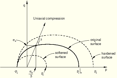
The yield surface of a crushable foam in the p–q (pressure stress–Mises equivalent stress) plane is illustrated in Figure 6–37.
The *CRUSHABLE FOAM, HARDENING=VOLUMETRIC option uses two data items to define the initial yield behavior.*CRUSHABLE FOAM, HARDENING=VOLUMETRIC 1.1, 0.1The first data item is the the ratio of initial yield stress in uniaxial compression to initial yield stress in hydrostatic compression,
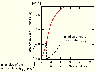
Include hardening effects with the *CRUSHABLE FOAM HARDENING option. The first data item on each line is the yield stress in uniaxial compression, given as a positive value; the second data item on each line is the absolute value of the corresponding plastic strain. The crushable foam hardening model follows the curve shown in Figure 6–38.
*CRUSHABLE FOAM HARDENING
0.22000E6, 0.0
0.24651E6, 0.1
0.27294E6, 0.2
0.29902E6, 0.3
0.32455E6, 0.4
0.34935E6, 0.5
0.37326E6, 0.6
0.39617E6, 0.7
0.41801E6, 0.8
0.43872E6, 0.9
0.45827E6, 1.0
0.49384E6, 1.2
0.52484E6, 1.4
0.55153E6, 1.6
0.57431E6, 1.8
0.59359E6, 2.0
0.62936E6, 2.5
0.65199E6, 3.0
0.68334E6, 5.0
0.68833E6, 10.0
Boundary conditions
Fully constrain the rigid surface representing the floor by applying a fixed boundary condition to the reference node, which you previously defined as node set REF.
*BOUNDARY
REF, ENCASTRE
Initial conditions
Give the circuit board and foam packaging an initial velocity of –4.43 m/s in the global 3-direction, corresponding to the velocity at the end of a 1 meter free fall.
*INITIAL CONDITIONS, TYPE=VELOCITY
BOARD, 3, -4.43
PACK, 3, -4.43
Defining contact
Either contact algorithm could be used for this problem. However, the definition of contact using the contact pair algorithm would be more cumbersome since, unlike general contact, the surfaces involved in contact pairs cannot span more than one body. We use the general contact algorithm in this example to demonstrate the simplicity of the contact definition for more complex geometries.
First, define a named contact property using the *SURFACE INTERACTION option, and specify a friction coefficient of 0.3.
*SURFACE INTERACTION, NAME=FRIC
*FRICTION
0.3,
Use the *CONTACT option to define a general contact interaction. Use the ALL ELEMENT BASED parameter on the *CONTACT INCLUSIONS option to specify self-contact for the unnamed, all-inclusive surface defined automatically by ABAQUS/Explicit. Use the *CONTACT PROPERTY ASSIGNMENT option to assign the contact property named FRIC to the general contact interaction.
*CONTACT
*CONTACT INCLUSIONS, ALL ELEMENT BASED
*CONTACT PROPERTY ASSIGNMENT
 , , FRIC
Use the *DYNAMIC, EXPLICIT option to select a dynamic stress/displacement analysis using explicit integration, and define the time period of the step as 20 ms using the following commands:
*STEP
*DYNAMIC, EXPLICIT
, 0.02
Output requests
Write the preselected field data to the output database file at 5 evenly spaced intervals during the analysis by including the following line in your input file:
*OUTPUT, FIELD, VARIABLE=PRESELECT, NUMBER INTERVAL=5Write values of nodal displacement (U), velocity (V), and acceleration (A) for each of the attached chips as history data to the output database file. In addition, write element values of logarithmic strain (LE), stress (S), principal stress (SP), and logarithmic principal strain (LEP) at the surfaces (section points 1 and 5) of the element set BOTPART of the circuit board to which the bottom-most chip is attached. Select an output interval of 0.1 ms.
*OUTPUT, HISTORY, TIME INTERVAL=0.1E-3
*NODE OUTPUT, NSET=CHIPS
U, V, A
*ELEMENT OUTPUT, ELSET=BOTPART
1, 5
LE, S, SP, LEP
Write energy values summed over the entire model. Specifically, write values for kinetic energy (ALLKE), internal energy (ALLIE), elastic strain energy (ALLSE), artificial energy (ALLAE), and the energy dissipated by plastic deformation (ALLPD).
*ENERGY OUTPUT
ALLIE, ALLKE, ALLPD, ALLAE, ALLSE
Indicate the end of the step with the *END STEP option.
Save your input in a file called circuit.inp. Run the analysis using the following command:
abaqus job=circuit analysisThis analysis is somewhat more complicated than the previous analyses in this guide, and it may take 45 minutes or more to run to completion, depending on the power of your computer.
Status file
Information concerning the initial stable time increment can be found at the top of the status file. The 10 most critical elements (i.e., those resulting in the smallest time increments) are also shown in rank order.
 -------------------------------------------------------------------------------
  MODEL INFORMATION (IN GLOBAL X-Y COORDINATES)
 -------------------------------------------------------------------------------

    Total mass in model = 3.49594E-02
    Center of mass of model = (-1.076768E-02, 4.948696E-02, 8.492264E-02)

     Moments of Inertia :
                  About Center of Mass              About Origin
       I(XX)          6.655609E-05                  4.042923E-04
       I(YY)          9.977436E-05                  3.559498E-04
       I(ZZ)          6.921255E-05                  1.588800E-04
       I(XY)         -1.344123E-05                  5.187227E-06
       I(YZ)         -5.240334E-06                 -1.521594E-04
       I(ZX)          3.958669E-05                  7.155425E-05

 -------------------------------------------------------------------------------
  STABLE TIME INCREMENT INFORMATION
 -------------------------------------------------------------------------------


   The stable time increment estimate for each element is based on
   linearization about the initial state.


    Initial time increment = 7.87965E-07

    Statistics for all elements:
       Mean = 1.04660E-05
       Standard deviation = 4.02486E-06

    Most critical elements :
     Element number   Rank    Time increment   Increment ratio
    ----------------------------------------------------------
           64          1       7.879647E-07      1.000000E+00
           83          2       7.879647E-07      1.000000E+00
           87          3       7.879647E-07      1.000000E+00
           42          4       7.879647E-07      9.999999E-01
           89          5       7.879647E-07      9.999999E-01
           97          6       7.879647E-07      9.999999E-01
           21          7       7.879648E-07      9.999999E-01
           30          8       7.879648E-07      9.999999E-01
           38          9       7.879648E-07      9.999999E-01
           39         10       7.879648E-07      9.999999E-01


  -------------------------------------------------------------------------------
  SOLUTION PROGRESS
 -------------------------------------------------------------------------------

  STEP 1  ORIGIN 0.00000E+00

   Total memory used for step 1 is approximately 926.5 kilowords
   Global time estimation algorithm will be used.
   Scaling factor :  1.0000
   Percentage change in total mass at the start of step: 0.00000E+00

             STEP      TOTAL       CPU     STABLE      CRITICAL  KINETIC
  INCREMENT  TIME      TIME        TIME   INCREMENT    ELEMENT   ENERGY
         0  0.000E+00 0.000E+00   00:00:00 7.488E-07      83   3.430E-01
 Results number  0 at increment zero.
 ODB Field Frame Number    0 of   5 requested intervals at increment zero.
      1154  1.001E-03 1.001E-03   00:01:55 8.375E-07      28   3.272E-01
                                   :
                                   :
                                   :
Start ABAQUS/Viewer by typing the following:
abaqus viewer odb=circuitat the operating system prompt.
Checking material directions
The material directions obtained from this orientation definition can be checked with ABAQUS/Viewer.
To plot the material orientation:
First, change the view to a more convenient setting. From the toolbar, click ![]() .
.
From the Views dialog box that appears, select the 1–3 setting.
From the main menu bar, select Plot![]() Material Orientations.
Material Orientations.
The orientations of the material directions of the circuit board at the end of the simulation are shown. The material directions are drawn in different colors. The material 1-direction is blue, the material 2-direction is yellow, and the 3-direction, if it is present, is red.
To view the initial material orientation, select Result![]() Step/Frame. In the Step/Frame dialog box that appears, select Increment 0. Click Apply.
Step/Frame. In the Step/Frame dialog box that appears, select Increment 0. Click Apply.
ABAQUS/Viewer displays the initial material directions.
To restore the display to the results at the end of the analysis, select the last increment available in the Step/Frame dialog box; and click OK.
Animation of results
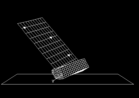
You will create a time-history animation of the deformation to help you visualize the motion and deformation of the circuit board and foam packaging during impact.
To create a time-history animation:
From the main menu bar, select Plot![]() Deformed Shape; or click
Deformed Shape; or click ![]() in the toolbox.
in the toolbox.
The deformed model shape at the end of the analysis appears.
Click Deformed Shape Plot Options in the prompt area.
The Deformed Shape Plot Options dialog box appears.
In this dialog box, choose the Hidden render style. Click OK.
From the main menu bar, select Animate![]() Time History.
Time History.
The animation controls appear in the prompt area, and the animation of the deformed model shape begins.
In the prompt area, click ![]() to stop the animation after a full cycle has been completed.
to stop the animation after a full cycle has been completed.
Change the animation options so that ABAQUS/Viewer swings through the animation at a faster rate.
From the main menu bar, select Options![]() Animation; or click Animation Options in the prompt area to open the Animation Options dialog box.
Animation; or click Animation Options in the prompt area to open the Animation Options dialog box.
Do the following:
Choose Swing.
Drag the frame rate slider to Fast.
Click OK, and replay the animation with these settings.
Plotting model energy histories
Plot graphs of various energy variables versus time. Since accelerations and reaction forces can change significantly from one increment to the next, it is important to plot time histories of these variables with enough data points to provide an accurate representation of the results.
To plot energy histories:
From the main menu bar, select Result![]() History Output.
History Output.
The History Output dialog box appears.
Select the ALLAE output variable, and save the data as Artificial Energy.
Select the ALLIE output variable, and save the data as Internal Energy.
Select the ALLKE output variable, and save the data as Kinetic Energy.
Select the ALLPD output variable, and save the data as Plastic Dissipation.
Select the ALLSE output variable, and save the data as Strain Energy.
Click Dismiss.
From the main menu bar, select Tools![]() XY Data
XY Data![]() Manager.
Manager.
The XY Data Manager dialog box appears.
In this dialog box, select all five curves and click Plot to view the X–Y plot.
The selected curves are plotted in the viewport.
Click Dismiss to close the dialog box.
Customize the appearance of the plot. Change the line styles of the curves, change the number of decimal places displayed on the X-axis, suppress the appearance of minor tick marks, and change the titles of the X- and Y-axes.
Click XY Curve Options in the prompt area.
The XY Curve Options dialog box appears.
In this dialog box, apply different line styles and thicknesses to each of the curves displayed in the viewport; then click Dismiss.
Click XY Plot Options in the prompt area.
The XY Plot Options dialog box appears.
In this dialog box:
Click the Axes tab, and set the number of decimal places to be displayed on the X-axis to zero.
Click the Tick Marks tab, and set the number of minor tick marks to be displayed on both axes equal to zero.
Click the Titles tab, and select user-specified title sources for both the X- and Y-axes. Enter an X-axis title of Time and a Y-axis title of Energy.
Click OK to apply the settings.
Now reposition the legend so that it appears inside the plot.
From the main menu bar, select Viewport![]() Viewport Annotation Options.
Viewport Annotation Options.
The Viewport Annotation Options dialog box appears.
Click the Legend tab, and enter a relative position of (50,75) for the upper left corner of the legend box in the viewport.
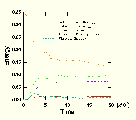
The energy histories appear as shown in Figure 6–40.
First, consider the kinetic energy history. At the beginning of the simulation the components are in free fall, and the kinetic energy is large. The initial impact deforms the foam packaging, thus reducing the kinetic energy. The components then rotate about the impacting corner until the side of the foam packaging impacts the floor at approximately 7 ms, further reducing the kinetic energy. The bodies remain in contact through most of the remainder of the simulation.
The deformation of the foam packaging during impact transfers energy from kinetic energy to internal energy in the foam packaging and the circuit board. From Figure 6–40 we can see that the internal energy increases as the kinetic energy decreases. In fact, the internal energy is composed of elastic energy and plastically dissipated energy, both of which are also plotted in Figure 6–40. Elastic energy rises to a peak and then falls as the elastic deformation recovers, but the plastically dissipated energy continues to rise as the foam is deformed permanently.
Another important energy output variable is the artificial energy, which is a substantial fraction (approximately 15%) of the internal energy in this analysis. By now you should know that the quality of the solution would improve if the artificial energy could be decreased to a smaller fraction of the total internal energy.
What causes high artificial strain energy in this problem?
In the example in Chapter 4, “Finite Elements and Rigid Bodies,” we saw that contact at a single node—such as the corner impact in this example—can cause hourglassing, especially in a coarse mesh. That example posed two methods of reducing the artificial strain energy: refining the mesh or rounding the impacting corner. For the current exercise, however, we shall continue with the original mesh, realizing that improving the mesh would lead to an improved solution.
Stresses and strains in the circuit board
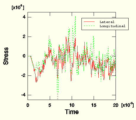
The next result we wish to examine is the stress and strain in the circuit board near the location of the chips. If the stress or strain under the components exceeds a limiting value, the solder securing the chips to the board will fail. Study the lateral and longitudinal stress histories at the top face (SPOS) of the element set BOTPART, which contains an element to which the bottom-most chip is attached.
To plot stress histories:
From the main menu bar, select Result![]() History Output.
History Output.
The History Output dialog box appears.
Select the S11 stress component on the SPOS surface of the element in element set BOTPART, and save the data as Lateral.
Select the S22 stress component on the SPOS surface of the element in element set BOTPART, and save the data as Longitudinal.
Click Dismiss.
From the main menu bar, select Tools![]() XY Data
XY Data![]() Manager.
Manager.
The XY Data Manager dialog box appears.
In this dialog box, select the two curves defined above; and click Plot to view the X–Y plot.
Click Dismiss to close the dialog box.
As before, customize the plot appearance to obtain a plot similar to Figure 6–41.
The stress plot shows that the longitudinal stress under the chip varies most of the time between –2 MPa and 2 MPa, with some peaks as large as –4 MPa; and the lateral stress follows a similar trend with less severe peaks. Both the lateral and the longitudinal stresses have peaks at approximately 7 ms. This point has been identified previously from the kinetic energy plot and animation as the instant at which the side of the packaging hits the floor.
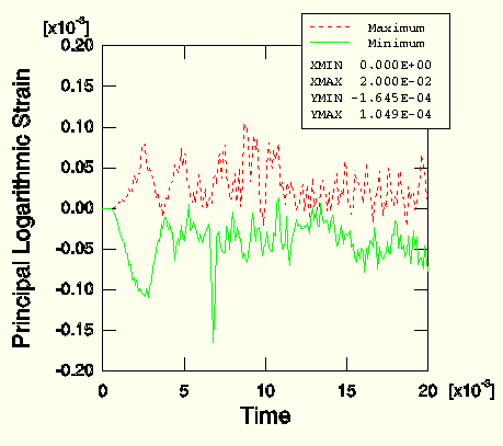
We wish to identify the peak strain in any direction. Therefore, the maximum and minimum principal logarithmic strains are of interest.
To plot logarithmic strain histories:
From the main menu bar, select Result![]() History Output.
History Output.
The History Output dialog box appears.
Select the principal logarithmic strain LEP1 on the SPOS surface of the element in element set BOTPART, and save the data as Minimum.
Select the principal logarithmic strain LEP2 on the SPOS surface of the element in element set BOTPART, and save the data as Maximum.
Click Dismiss to close the dialog box.
From the main menu bar, select Tools![]() XY Data
XY Data![]() Manager.
Manager.
The XY Data Manager dialog box appears.
In the dialog box, select the two curves defined above; and click Plot to view the X–Y plot.
The settings of the previous plot remain in effect and are inappropriate for this plot. Change the settings to make this X–Y plot more useful, as shown in Figure 6–42.
The strain curves show peak and decay behavior similar to that of the stresses. The peak values are approximately 0.015% compressive and 0.01% tensile.
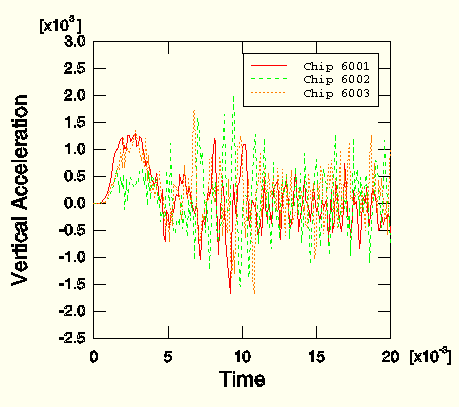
Acceleration and velocity histories at the chips
Another result that may assist us in determining the desirability of the foam packaging is the acceleration and velocity of the chips attached to the circuit board. Excessive accelerations during impact may damage the chips, even though they may remain attached to the circuit board. Therefore, we need to plot the acceleration histories of the three chips. Since we expect the accelerations to be greatest in the 3-direction, we plot the variable A3.
To plot acceleration histories:
From the main menu bar, select Result![]() History Output.
History Output.
The History Output dialog box appears.
Select the acceleration A3 of the nodes in node set Chips, and save the three X–Y data objects as Chip 6001, Chip 6002, and Chip 6003. If you used the input file listed in “Circuit board drop test,” Section A.7, these correspond to nodes 60, 357, and 403, respectively.
Click Dismiss.
From the main menu bar, select Tools![]() XY Data
XY Data![]() Manager.
Manager.
The XY Data Manager dialog box appears.
In this dialog box, select the three curves created above; and click Plot.
The X–Y plot appears in the viewport. As before, customize the plot appearance to obtain a plot similar to Figure 6–43.
The acceleration of chip 6001, which is at the top of the board, is smooth compared to the accelerations of the other chips early in the simulation and reaches a peak at approximately 2 ms. However, for chip 6002 the peak acceleration is 2000 m/s2 at approximately 10 ms, while for chip 6003 the peak acceleration is 1750 m/s2 at approximately 7 ms, the instant at which the side of the packaging impacts the floor. This result may be accentuated by the board's rotation following the initial impact.
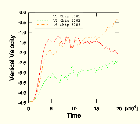
The final plot, Figure 6–44, shows how the three chips change velocity during impact.
At the beginning of the simulation, the chips all have the same downward velocity after the 1 meter drop. The chips all decelerate following the initial impact; but as the board rotates, the velocity profiles diverge rapidly. Only the component near the base of the board, chip 6003, approaches a zero velocity at the end of the analysis.To plot velocity histories:
From the main menu bar, select Result![]() History Output.
History Output.
The History Output dialog box appears.
Select the velocity V3 of the nodes in node set Chips, and save the X–Y data objects as V3 Chip 6001, V3 Chip 6002, and V3 Chip 6003. If you used the input file listed in “Circuit board drop test,” Section A.7, these correspond to nodes 60, 357, and 403, respectively.
Click Dismiss to close the dialog box.
From the main menu bar, select Tools![]() XY Data
XY Data![]() Manager.
Manager.
The XY Data Manager dialog box appears.
In this dialog box, select the three curves defined above; and click Plot.
The X–Y plot is shown in the viewport. As before, customize the plot appearance to obtain a plot similar to Figure 6–44.