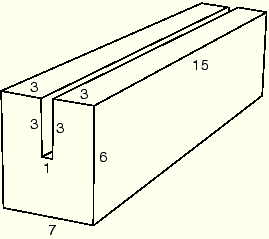
In this example you will investigate the behavior of a circuit board in protective crushable foam packaging dropped at an angle onto a rigid surface. Your goal is to assess whether the foam packaging is adequate to prevent circuit board damage when the board is dropped from a height of 1 meter. You will use the general contact capability in ABAQUS/Explicit to model the interactions between the different components. Figure 12–48 shows the dimensions of the circuit board and foam packaging in millimeters and the material properties.
Create the model for this simulation with ABAQUS/CAE. A Python script is provided in “Circuit board drop test,” Section A.13. When this script is run through ABAQUS/CAE, it creates the complete analysis model for this problem. Run this script if you encounter difficulties following the instructions given below or if you wish to check your work. Instructions on how to fetch and run the script are given in Appendix A, “Example Files.”
If you do not have access to ABAQUS/CAE or another preprocessor, the input file required for this problem can be created manually, as discussed in “Example: circuit board drop test,” Section 6.4 of Getting Started with ABAQUS/Explicit: Keywords Version.
Defining the model geometry
You will create three parts representing the packaging, the circuit board, and the floor. The chips will be represented using discrete point masses. You will also create a number of datum points to aid in positioning the part instances and the point masses.
To define the packaging geometry:
The packaging is a three-dimensional solid structure. Create a three-dimensional, deformable part with an extruded solid base feature to represent the packaging; name the part Packaging. Use an approximate part size of 0.1, and sketch a 0.02 m × 0.024 m rectangle as the profile. Specify 0.11 m as the extrusion depth.
From the main menu bar, select Shape![]() Cut
Cut![]() Extrude to create the cut in the packaging in which the circuit board will rest.
Extrude to create the cut in the packaging in which the circuit board will rest.
Select the left end of the packaging as the plane for the extruded cut. Select a vertical line on the packaging profile to be vertical and on the right in the sketching plane.
In the Sketcher, create a vertical construction line through the center of the packaging. Apply a fixed constraint to the construction line.
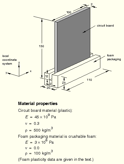
Sketch the profile of the cut shown in Figure 12–49. Use a Symmetry constraint to center the cut about the construction line and edit the dimensions of the cut profile so that it is 0.002 m wide and extends a distance of 0.012 m into the packaging.
In the Edit Cut Extrusion dialog box that appears upon completion of the sketch, select Through All as the end condition and select the arrow direction representing a cut into the packaging.
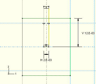
Create a datum point centered on the bottom face of the cut, as shown in Figure 12–50. This point will be used to position the board relative to the packaging.
From the main menu bar, select Tools![]() Datum.
Datum.
The Create Datum dialog box appears.
Accept the default selection of Point as the datum type, select Midway between 2 points as the method, and click OK.
Select the two points centered on the bottom face at either end of the cut to be the two points between which the datum point will be created.
ABAQUS/CAE creates the datum point shown in Figure 12–50.
To define the circuit board geometry:
The circuit board can be modeled as a thin, flat plate with chips attached to it. Create a three-dimensional, deformable planar shell to represent the circuit board; name the part Board. Use an approximate part size of 0.5, and sketch a 0.100 m × 0.150 m rectangle for the profile.
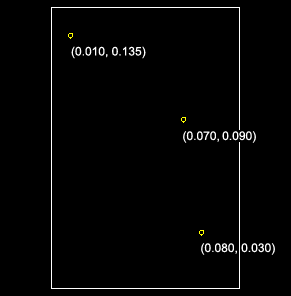
Create the three datum points shown in Figure 12–51. These points will be used to position the chips on the board.
Figure 12–51 Datum points used to position the chips relative to the board. Numbers in parentheses are (x, y) coordinates in meters based on a local origin at the bottom left corner of the circuit board.
From the main menu bar, select Tools![]() Datum.
Datum.
The Create Datum dialog box appears.
Accept the default selection of Point as the datum type, select Offset from point as the method, and click Apply.
Select the bottom left corner of the board as the point from which to offset, and enter the coordinates for one of the points shown in Figure 12–51.
Repeat Steps b and c to create the other two datum points.
To define the floor:
The surface that the circuit board will impact is effectively rigid. Create a three-dimensional, discrete rigid planar shell to represent the floor; name the part Floor. Use an approximate part size of 0.5. The rigid surface should be large enough to keep any deformable bodies from falling off the edges.
Sketch a 0.2 m × 0.2 m square as the profile. To simplify the positioning of parts in the assembly of the model, ensure that the center of the surface corresponds to point (0, 0) in the sketcher. This also corresponds to the origin of the global coordinate system.
Assign a reference point at the center of the part.
Defining the material and section properties
The circuit board is assumed to be made of a PCB elastic material with a Young's modulus of 45 × 109 Pa and a Poisson's ratio of 0.3. The mass density of the board is 500 kg/m3. Define a material named PCB with these properties.
The foam packaging material will be modeled using the crushable foam plasticity model. The elastic properties of the packaging include a Young's modulus of 3 × 10⁶ Pa and a Poisson's ratio of 0.0. The material density of the packaging is 100.0 kg/m3. Define a material named Foam with these properties; do not close the material editor.
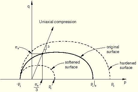
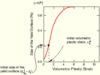
The yield surface of a crushable foam in the p–q (pressure stress-Mises equivalent stress) plane is illustrated in Figure 12–52.
The initial yield behavior is governed by the ratio of initial yield stress in uniaxial compression to initial yield stress in hydrostatic compression,Hardening effects are also included in the material model definition. Table 12–3 summarizes the yield stress–plastic strain data.
Table 12–3 Yield stress–plastic strain data for the crushable foam model.
| Yield stress in uniaxial compression (Pa) | Plastic strain |
|---|---|
| 0.22000E6 | 0.0 |
| 0.24651E6 | 0.1 |
| 0.27294E6 | 0.2 |
| 0.29902E6 | 0.3 |
| 0.32455E6 | 0.4 |
| 0.34935E6 | 0.5 |
| 0.37326E6 | 0.6 |
| 0.39617E6 | 0.7 |
| 0.41801E6 | 0.8 |
| 0.43872E6 | 0.9 |
| 0.45827E6 | 1.0 |
| 0.49384E6 | 1.2 |
| 0.52484E6 | 1.4 |
| 0.55153E6 | 1.6 |
| 0.57431E6 | 1.8 |
| 0.59359E6 | 2.0 |
| 0.62936E6 | 2.5 |
| 0.65199E6 | 3.0 |
| 0.68334E6 | 5.0 |
| 0.68833E6 | 10.0 |
Define a homogeneous shell section named BoardSection that refers to the material PCB. Specify a thickness of 0.002 m, and assign this section definition to the part Board. Define a homogeneous solid section named FoamSection that refers to the material Foam. Specify a thickness of 1.0 m, and assign this section definition to the part Packaging.
For the circuit board it is most meaningful to output stress results in the longitudinal and lateral directions, aligned with the edges of the board. Therefore, you need to specify a local material orientation for the circuit board mesh.
To specify a material orientation for the board:
Double-click Board underneath the Parts container in the Model Tree.
To define a datum coordinate system for the orientation:
From the main menu bar, select Tools![]() Datum.
Datum.
Select CSYS as the type and 2 lines as the method, and click OK.
In the Create Datum CSYS dialog box that appears, select a rectangular coordinate system and click Continue.
In the viewport, select the bottom horizontal edge of the board to be the local x-axis and the right vertical edge of the board to lie in the X–Y plane.
The datum coordinate system appears in yellow in the viewport.
From the main menu bar of the Property module, select Assign![]() Material Orientation. In the viewport select the circuit board. Select the datum coordinate system as the coordinate system. In the prompt area select Axis–3 as the shell surface normal; enter 0.0 as the additional rotation about that axis.
Material Orientation. In the viewport select the circuit board. Select the datum coordinate system as the coordinate system. In the prompt area select Axis–3 as the shell surface normal; enter 0.0 as the additional rotation about that axis.
The material orientation appears on the board in the viewport. Click OK in the prompt area.
Creating the assembly
In the Model Tree, double-click Instances underneath the Assembly container and create a dependent instance of the floor.
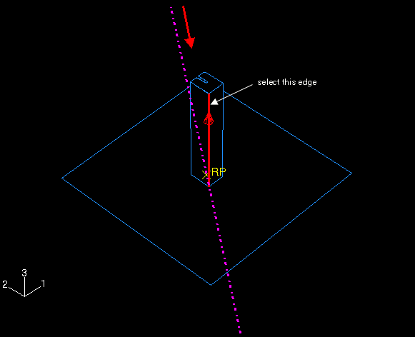
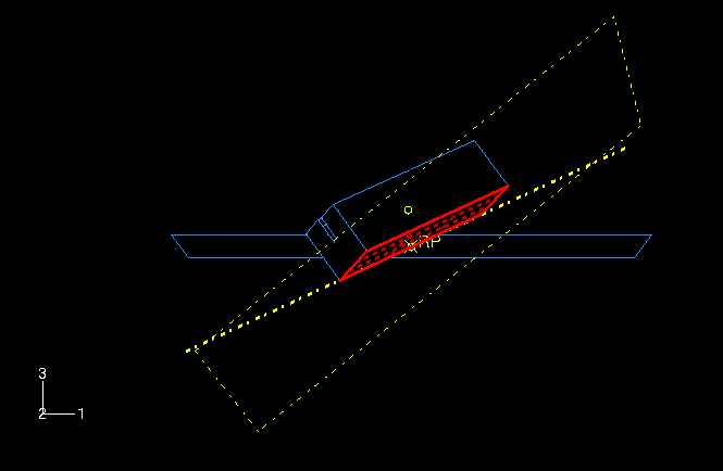
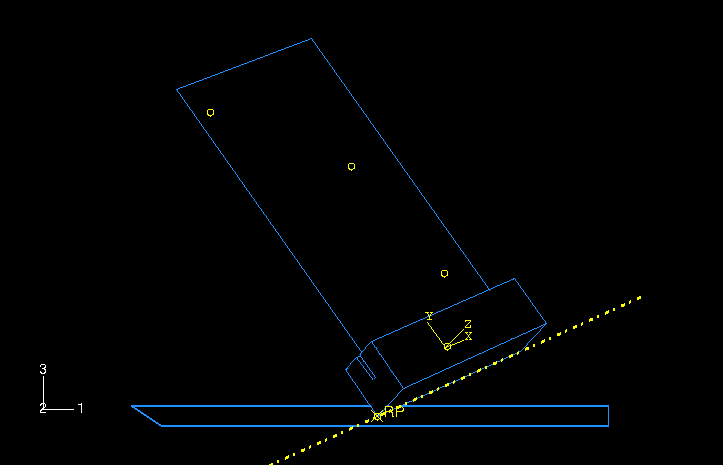
The circuit board will be dropped at an angle; the final model assembly is shown in Figure 12–54.
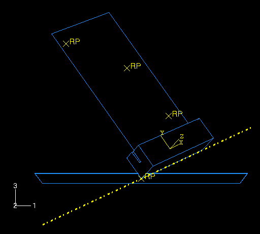
You will use the positioning tools in the Assembly module to position the packaging first; then you will position the board relative to the packaging. Finally, you will create a reference point at each datum point location of the board to represent the chips.To position the packaging:
From the main menu bar of the Assembly module, select Tools![]() Datum to create additional datum points that will help you position the packaging.
Datum to create additional datum points that will help you position the packaging.
Select Point as the type, select Enter coordinates as the method, and click Apply.
Create two datum points at (0, 0, 0) and (0.5, 0.707, 0.25).
Click the auto-fit tool to see both points in the viewport.
In the Create Datum dialog box, select Axis as the type, select 2 points as the method, and click Apply. Create a datum axis defined by the two datum points created in the previous step.
Tip: Suppress the display of the reference points in the viewport to select the datum point located at (0, 0, 0).
Instance the packaging.
Constrain the packaging so that the bottom edge aligns with the datum axis.
From the main menu bar, select Constraint![]() Edge to Edge.
Edge to Edge.
Select the edge of the packaging shown in Figure 12–55 as a straight edge of the movable instance.
Tip:
To obtain a better view of the model, select View![]() Specify from the main menu bar and select Viewpoint as the method; enter (–1, –1, 1) for the viewpoint vector and (0, 0, 1) for the up vector.
Specify from the main menu bar and select Viewpoint as the method; enter (–1, –1, 1) for the viewpoint vector and (0, 0, 1) for the up vector.
Select the datum axis as the fixed instance.
If necessary, click Flip in the prompt area to reverse the direction of the arrow on the packaging; click OK when the arrows point in opposite directions as shown in Figure 12–55.
Tip: You may need to zoom out and rotate the model to see the arrow on the datum axis. The direction of this arrow depends on how you defined the axis initially; if the arrow on your axis points in the reverse direction of the one shown in the figure, the arrow on your packaging should also be opposite to the figure.
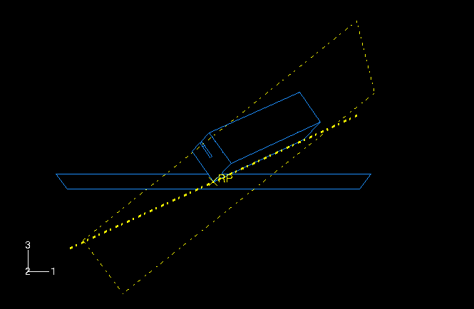
ABAQUS/CAE positions the packaging as shown in Figure 12–56.
Note: ABAQUS/CAE stores position constraints as features of the assembly; if you make a mistake while positioning the assembly, you can delete the position constraints. Simply click mouse button 3 on the constraint you wish to delete in the list of Position Constraints items found underneath the Assembly container in the Model Tree, and select Delete from the menu that appears.
Create a third datum point at (–0.5, 0.707, –0.5), and click the auto-fit tool again.
In the Create Datum dialog box, select Plane as the type, select Line and point as the method, and click Apply. Create a datum plane defined by the datum axis created earlier and the datum point created in the previous step.
Constrain the packaging so that the bottom face lies on the datum plane.
From the main menu bar, select Constraint![]() Face to Face.
Face to Face.
Select the face of the packaging shown in Figure 12–57 as a face of the movable instance.
Select the datum plane as the fixed instance.
If necessary, click Flip in the prompt area; click OK when both arrows point in the same direction.
Accept the default distance of 0.0 from the fixed plane.
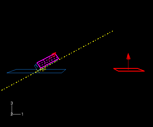
Finally, constrain the packaging to contact the floor at its center.
From the main menu bar, select Constraint![]() Coincident Point.
Coincident Point.
Select the lowest vertex of the packaging as a point on the movable instance, and select the reference point on the floor as a point on the fixed instance.
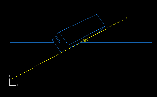
ABAQUS/CAE positions the packaging as shown in Figure 12–58.
Now, translate the floor slightly downward to ensure that there is no initial overclosure between the packaging and the floor.
Convert the relative position constraints to absolute constraints to avoid conflicts. From the main menu bar, select Instance![]() Convert Constraints. Select the packaging in the viewport, and click Done in the prompt area.
Convert Constraints. Select the packaging in the viewport, and click Done in the prompt area.
From the main menu bar, select Instance![]() Translate.
Translate.
Select the floor in the viewport.
Enter (0.0, 0.0, 0.0) as the start point for the translation vector and (0.0, 0.0, –0.0001) as the end point for the translation vector.
Click OK to accept the new position.
To position the circuit board:
Instance the circuit board. In the Create Instance dialog box, toggle on Auto-offset from other instances.
From the main menu bar, select Constraint![]() Parallel Face. Select the face of the board as a face on the movable instance; select a face on the long side of the packaging as a face on the fixed instance. If necessary, click Flip in the prompt area to ensure that the arrows on both faces point in the directions shown in Figure 12–59; click OK to complete the constraint.
Parallel Face. Select the face of the board as a face on the movable instance; select a face on the long side of the packaging as a face on the fixed instance. If necessary, click Flip in the prompt area to ensure that the arrows on both faces point in the directions shown in Figure 12–59; click OK to complete the constraint.
From the main menu bar, select Constraint![]() Parallel Edge. Select the top edge of the board as an edge on the movable instance. Select an edge along the length of the packaging as an edge on the fixed instance. If necessary, click Flip in the prompt area to ensure that the arrows on both edges point in the same direction, as shown in Figure 12–60; click OK to complete the constraint.
Parallel Edge. Select the top edge of the board as an edge on the movable instance. Select an edge along the length of the packaging as an edge on the fixed instance. If necessary, click Flip in the prompt area to ensure that the arrows on both edges point in the same direction, as shown in Figure 12–60; click OK to complete the constraint.
From the main menu bar, select Constraint![]() Coincident Point. Select the midpoint of the bottom of the board as a point on the movable instance. Select the datum point at the center of the cut in the packaging as a point on the fixed instance.
Coincident Point. Select the midpoint of the bottom of the board as a point on the movable instance. Select the datum point at the center of the cut in the packaging as a point on the fixed instance.
Tip: Set the render style to hidden to facilitate your selection of the datum point.
Figure 12–61 shows the final position of the circuit board. The circuit board and the slot in the packaging are the same thickness (2 mm) so there is a snug fit between the two bodies.
To create the chips:
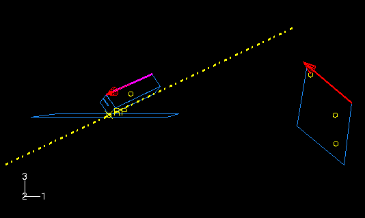
Create a reference point at each of the three datum point locations on the board to represent each chip. Each of these reference points will later be assigned mass properties. To create a reference point, select Tools![]() Reference Point from the main menu bar of the Assembly module.
Reference Point from the main menu bar of the Assembly module.
Once you have created the reference points, the assembly is complete.
TopChip for the reference point of the top chip
MidChip for the reference point of the middle chip
BotChip for the reference point of the bottom chip
BotBoard for the bottom edge of the board
Defining the step and requesting output
Create a single dynamic, explicit step named Drop; set the time period to 0.02 s. Accept the default history and field output requests. In addition, request vertical velocity (V3), and vertical acceleration (A3) history output every 0.1 × 10⁻³ s for each of the three chips.
Tip: Define the history output request for the first chip; using the History Output Requests Manager, copy the request and edit the domain to define the requests for the other chips.
Defining contact
Either contact algorithm in ABAQUS/Explicit could be used for this problem. However, the definition of contact using the contact pair algorithm would be more cumbersome since, unlike general contact, the surfaces involved in contact pairs cannot span more than one body. We use the general contact algorithm in this example to demonstrate the simplicity of the contact definition for more complex geometries.
Define a contact interaction property named Fric. In the Edit Contact Property dialog box, select Mechanical![]() Tangential Behavior; select Penalty as the friction formulation; and specify a friction coefficient of 0.3 in the table. Accept all other defaults.
Tangential Behavior; select Penalty as the friction formulation; and specify a friction coefficient of 0.3 in the table. Accept all other defaults.
Create a General contact (Explicit) interaction named All in the Drop step. In the Edit Interaction dialog box, accept the default selection of All* with self for the Contact Domain to specify self-contact for the default unnamed, all-inclusive surface defined automatically by ABAQUS/Explicit. This is the simplest way to define contact in ABAQUS/Explicit for an entire model. Accept Fric as the Global property assignment, and click OK.
Defining tie constraints
You will use tie constraints to attach the chips to the board. Begin by defining a surface named Board for the circuit board. Select Both sides in the prompt area to specify that the surface is double-sided. In the Model Tree, double-click the Constraints container; define a tie constraint named TopChip. Select Board as the master surface and TopChip as the slave node region. Toggle off Tie rotational DOFs if applicable in the Edit Constraint dialog box since only the effects of the chip masses are of interest, and click OK. Yellow circles appear on the model to represent the constraint. Similarly, create tie constraints named MidChip and BotChip for the middle and bottom chips.
Assigning mass properties to the chips:
You will assign a point mass to each chip. To do this, expand Engineering Features underneath the Assembly container in the Model Tree. In the list that appears, double-click Inertias. In the Create Inertia dialog box, enter the name TopChipMass and click Continue. Select the set TopChip, and assign it a mass of 0.005 kg. Repeat this procedure for the two remaining chips.
Specifying loads and boundary conditions
Constrain the reference point on the floor in all directions; for example, you could prescribe an ENCASTRE boundary condition.
Two methods could be used to simulate the circuit board being dropped from a height of 1 m. You could model the circuit board and foam at a height of 1 m above the floor and allow ABAQUS/Explicit to calculate the motion under the influence of gravity; however, this method is impractical because of the large number of increments required to complete the “free-fall” part of the simulation. The more efficient method is to model the circuit board and packaging in an initial position very close to the surface of the floor (as you have done in this problem) and specify an initial velocity of 4.439 m/s to simulate the 1 m drop. Create a predefined field in the initial step to specify an initial velocity of V3 = –4.43 m/s for the board, chips, and packaging.
Meshing the model and defining a job
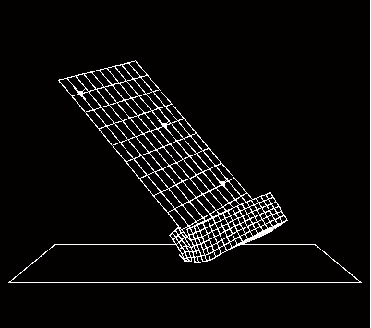
Seed the circuit board with 10 elements along its length and height. Seed the edges of the packaging as shown in Figure 12–62.
The mesh for the packaging will be too coarse near the impacting corner to provide highly accurate results; however, it will be adequate for a low-cost preliminary study. Using the swept mesh technique, mesh the board with S4R elements and the packaging with C3D8R elements from the ABAQUS/Explicit library. Use enhanced hourglass control for the packaging mesh to control hourglassing effects. Specify a global seed of 1.0 for the floor, and mesh it with one ABAQUS/Explicit R3D4 element.Note: The suggested mesh density exceeds the model size limits of the ABAQUS Student Edition. Specify 12 elements along the length of the foam packaging if using this product.
Create a job named Circuit and give it the following description: Circuit board drop test. Double precision should be used for this analysis to minimize the noise in the solution. In the Precision tabbed page of the job editor, select Double as the ABAQUS/Explicit precision. Save your model to a model database file, and submit the job for analysis. Monitor the solution progress; correct any modeling errors that are detected, and investigate the cause of any warning messages.
Enter the Visualization module, and open the output database file created by this job (Circuit.odb).
Checking material directions
The material directions obtained from the orientation definition can be checked in the Visualization module.
To plot the material orientation:
First, change the view to a more convenient setting. From the toolbar, click ![]() .
.
From the Views dialog box that appears, select the 1–3 setting.
From the main menu bar, select Plot![]() Material Orientations
Material Orientations![]() On Deformed Shape.
On Deformed Shape.
The orientations of the material directions for the circuit board at the end of the simulation are shown. The material directions are drawn in different colors. The material 1-direction is blue, the material 2-direction is yellow, and the 3-direction, if it is present, is red.
To view the initial material orientation, select Result![]() Step/Frame. In the Step/Frame dialog box that appears, select Increment 0. Click Apply.
Step/Frame. In the Step/Frame dialog box that appears, select Increment 0. Click Apply.
ABAQUS displays the initial material directions.
To restore the display to the results at the end of the analysis, select the last increment available in the Step/Frame dialog box; and click OK.
Animation of results
You will create a time-history animation of the deformation to help you visualize the motion and deformation of the circuit board and foam packaging during impact.
To create a time-history animation:
Plot the deformed model shape at the end of the analysis.
From the main menu bar, select Animate![]() Time History.
Time History.
The animation of the deformed model shape begins.
In the context bar, click ![]() to pause the animation after a full cycle has been completed.
to pause the animation after a full cycle has been completed.
Change the animation options so that ABAQUS swings through the animation:
From the main menu bar, select Options![]() Animation to open the Animation Options dialog box.
Animation to open the Animation Options dialog box.
Choose Swing.
Click OK, and replay the animation with these settings.
Plotting model energy histories
Plot graphs of various energy variables versus time. Since accelerations and reaction forces can change significantly from one increment to the next, it is important to plot time histories of these variables with enough data points to provide an accurate representation of the results.
To plot energy histories:
In the Results Tree, expand the History Output sub-containers for the output database named Circuit.odb.
Select the ALLAE output variable, and save the data as Artificial Energy.
Select the ALLIE output variable, and save the data as Internal Energy.
Select the ALLKE output variable, and save the data as Kinetic Energy.
Select the ALLPD output variable, and save the data as Plastic Dissipation.
Select the ALLSE output variable, and save the data as Strain Energy.
In the Results Tree, expand the XYData container.
Select all five curves. Click mouse button 3, and select Plot from the menu that appears to view the X–Y plot.
The selected curves are plotted in the viewport.
Customize the appearance of the plot. Change the line styles of the curves, change the number of decimal places displayed on the X-axis, suppress the appearance of minor tick marks, and change the titles of the X- and Y-axes.
Open the XY Curve Options dialog box.
In this dialog box, apply different line styles and thicknesses to each of the curves displayed in the viewport.
Open the XY Plot Options dialog box.
In this dialog box:
Click the Axes tab, and set the number of decimal places to be displayed on the X-axis to zero.
Click the Tick Marks tab, and set the number of minor tick marks to be displayed on both axes equal to zero.
Click the Titles tab, and select user-specified title sources for both the X- and Y-axes. Enter an X-axis title of Time and a Y-axis title of Energy.
Click OK to apply the settings.
Now reposition the legend so that it appears inside the plot.
From the main menu bar, select Viewport![]() Viewport Annotation Options.
Viewport Annotation Options.
The Viewport Annotation Options dialog box appears.
Click the Legend tab, and enter a relative position of (50, 75) for the upper left corner of the legend box in the viewport.
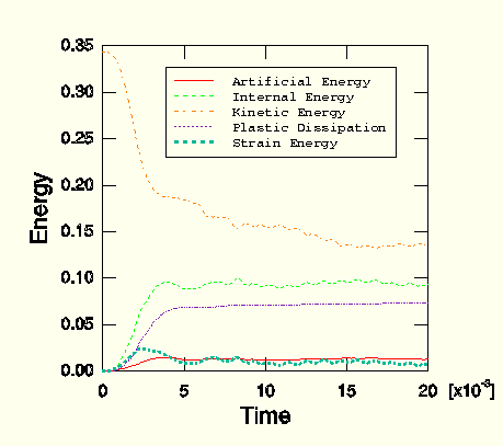
The energy histories appear as shown in Figure 12–64.
First, consider the kinetic energy history. At the beginning of the simulation the components are in free fall, and the kinetic energy is large. The initial impact deforms the foam packaging, thus reducing the kinetic energy. The components then rotate about the impacting corner until the side of the foam packaging impacts the floor at approximately 7 ms, further reducing the kinetic energy. The bodies remain in contact through most of the remainder of the simulation.
The deformation of the foam packaging during impact transfers energy from kinetic energy to internal energy in the foam packaging and the circuit board. From Figure 12–64 we can see that the internal energy increases as the kinetic energy decreases. In fact, the internal energy is composed of elastic energy and plastically dissipated energy, both of which are also plotted in Figure 12–64. Elastic energy rises to a peak and then falls as the elastic deformation recovers, but the plastically dissipated energy continues to rise as the foam is deformed permanently.
Another important energy output variable is the artificial energy, which is a substantial fraction (approximately 15%) of the internal energy in this analysis. Usually the artificial energy should be kept to a small fraction of the internal energy. The exception to this rule is when the artificial energy is due to enhanced hourglass control. This method of hourglass control accounts for real (physical) energy in the analysis. Thus, the high value of artificial energy in this problem is not a concern.
Stresses and strains in the circuit board
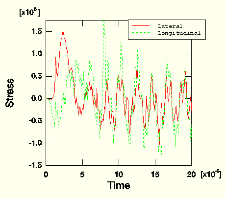
The next result we wish to examine is the stress and strain in the circuit board near the location of the chips. If the stress or strain under the components exceeds a limiting value, the solder securing the chips to the board will fail. Study the lateral and longitudinal stress histories at the top face (SPOS) of the element set BotBoard, which contains elements in the vicinity of the bottom-most chip.
To plot stress histories:
In the History Output container of the Results Tree, select the S11 stress component on the SPOS surface of any element in set BotBoard, and save the data as Lateral .
Select the S22 stress component on the SPOS surface of the same element in set BotBoard, and save the data as Longitudinal.
In the Results Tree, select the two curves defined above underneath the XYData container and plot them.
As before, customize the plot appearance to obtain a plot similar to Figure 12–65. The actual plot will depend on which element you selected.
The stress plot in Figure 12–65 shows that the longitudinal stress near the bottom chip varies most of the time between –1 MPa and 1 MPa, with some peaks as large as 2 MPa; and the lateral stress follows a similar trend with less severe peaks. The longitudinal stress peaks at approximately 7 ms. This point has been identified previously from the kinetic energy plot and animation as the instant at which the side of the packaging hits the floor.
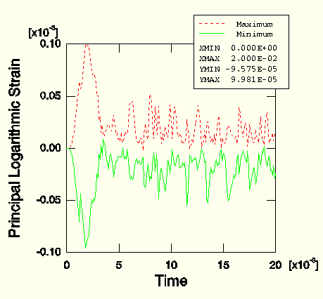
We wish to identify the peak strain in any direction. Therefore, the maximum and minimum principal logarithmic strains are of interest.
To plot logarithmic strain histories:
In the History Output container of the Results Tree, select the principal logarithmic strain LEP1 on the SPOS surface of the same element in set BotBoard, and save the data as Minimum.
Select the principal logarithmic strain LEP2 on the SPOS surface of the same element in set BotBoard, and save the data as Maximum.
Plot the two curves defined above.
The settings of the previous plot remain in effect and are inappropriate for this plot. Change the settings to make this X–Y plot more useful, as shown in Figure 12–66.
The strain curves show peak and decay behavior similar to that of the stresses. The peak values are approximately 0.01% compressive and 0.01% tensile.
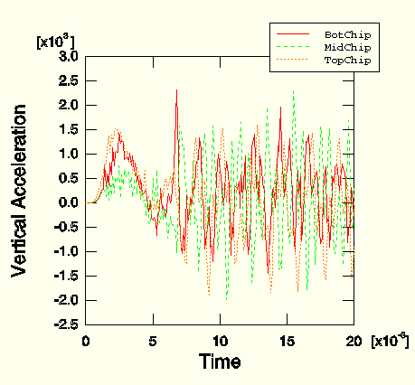
Acceleration and velocity histories at the chips
Another result that may assist us in determining the desirability of the foam packaging is the acceleration and velocity of the chips attached to the circuit board. Excessive accelerations during impact may damage the chips, even though they may remain attached to the circuit board. Therefore, we need to plot the acceleration histories of the three chips. Since we expect the accelerations to be greatest in the 3-direction, we plot the variable A3.
To plot acceleration histories:
In the History Output container of the Results Tree, select the acceleration A3 of the nodes in sets TopChip, MidChip, and BotChip; and plot the three X–Y data objects.
The X–Y plot appears in the viewport. As before, customize the plot appearance to obtain a plot similar to Figure 12–67.
The acceleration of TopChip, which is at the top of the board, is smooth compared to the accelerations of the other chips early in the simulation and reaches a peak at approximately 2 ms. However, for MidChip the peak acceleration is 2300 m/s2 at approximately 15 ms, while for BotChip the peak acceleration is 2300 m/s2 at approximately 7 ms, the instant at which the side of the packaging impacts the floor. This result may be accentuated by the board's rotation following the initial impact.
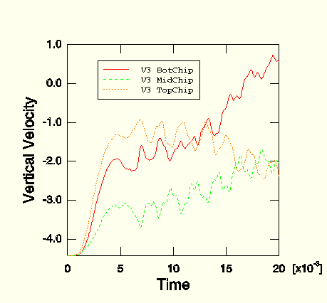
The final plot, Figure 12–68, shows how the three chips change velocity during impact. At the beginning of the simulation, the chips all have the same downward velocity after the 1 meter drop. The chips all decelerate following the initial impact; but as the board rotates, the velocity profiles diverge rapidly. Only the component near the base of the board, BotChip, approaches a zero velocity at the end of the analysis.
To plot velocity histories:
In the History Output container of the Results Tree, select the velocity V3 of the nodes in sets TopChip, MidChip, and BotChip; and plot the X–Y data objects.
The X–Y plot is shown in the viewport. As before, customize the plot appearance to obtain a plot similar to Figure 12–68.