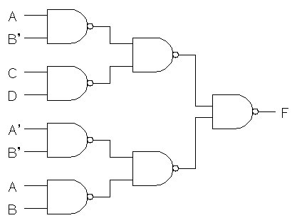
- 1. For the circuit below find the delay from each input to the output using the following methods:
- A. Find tphl and tplh for each path assuming the
propagation for each gate is tphl = 0.3 nS and tplh = 0.5 nS.
From these values, find tpd for each path (tpd is the average of
tphl and tplh).
- B. Use an average propagation delay, tpd = 0.4 nS, for each gate.
- C. Compare the answers in parts A and B and discuss any differences.

- 2. Develop a decimal Gray code sequence (starting at binary value
00002) that goes from 0 to 9. Make sure that only one bit
changes when rolling over from 9 to 0.
- A. Show a truth table of the decimal Gray code.
- B. Design a circuit to convert a binary value to the decimal Gray
code.
- C. Design a circuit that has a decimal Gray code input and
generates an error if the input is an invalid binary combination.
- D. Write a VHDL description of both circuits. Simulate the VHDL
description.
- 3. Design a combinational circuit that accepts a 4-bit number and
generates a 4-bit binary number output that approximates the following
function:
X = 8*sin(Y*5.625)
Where Y is the input to the circuit and X is the output. Make sure that you
round up or down as appropriate for the output. The sine argument is in
degrees (the argument ranges from 0 to 84.375 degrees in increments of 5.625
degrees). Don't draw a circuit. Work the problem until you have
sum-of-product or product-of-sums equations.
- 4. For the following equation below:
- A. Draw the circuit for the equation without simplifying:
- B. Use manual analysis to create a truth table for the circuit.
- C. Write a VHDL description of the circuit and verify the truth table from
part B by simulating the circuit with each possible input combination.
F = (C(A' + B) + (BD)')' + (C + B)'
- 5. Design a 4-to-16 line decoder with enable using 2-to-4 line decoders
with enable.
- 6. Design a circuit to implement the decimal Gray code error signal,
from problem 2C, using a decoder and one OR gate.
- 7. Implement the following equations using a PAL. Show the fuse map
and programming table.
X = BC + B'C'D'
Y = AC'D' + BC'D + AB + BCD'
Z = A'B'C' + B'C'D' + ABC'D + BCD'
- 8. Implement the following equations using a PLA. Show the fuse map
and programming table.
F1 = A'B' + A'C' + ABC
F2 = AB' + AC' + A'BC
- 9. Design a 16-to-1 multiplexer using 4-to-1 mulitplexers.
- 10. Implement the following Boolean function using a multiplexer and one
inverter.
F(A,B,C,D) = SUMm(1,2,5,6,7,8)
- 11. Design a 7-to-1 multiplexer using two 4-to-1 multiplexers and the
minimum amount of additional combinational logic.
- 12. Design an 8-to-3 priority encoder using 4-to-2 priority encoders
and the minimum amount of additional combinational logic.
- 13. Design a 2's complementer cell. The cells are connected
in cascade with lines similar to carry signals connected between them.
The value applied to the least significant cell's Cin is 0.
- 14. To speed up the circuit in the previous problem, design a
lookahead-like circuit for a 4-bit 2's complementer circuit that uses four
2's complementer cells.
- 15. From the previous two problems, write the following VHDL
descriptions:
- A. 2's complementer cell.
- B. The look-ahead circuit.
- C. A four-bit 2's complementer circuit using the VHDL descriptions
of A and B as components.
Simulate your design to verify that the circuit functions correctly.
- 16. Design a combinational circuit cell used for comparing two
unsigned numbers A and B to see if B is greater than A. The cells are
connected together in cascade with carry-like signals.
- 17. Draw a circuit that implements the equation Z = A * (B + C).
A, B, and C are 2-bit unsigned numbers. The number of bits for Z is
large enough to contain the result of the statement. Use half adders,
full adders, and AND gates.
- 18. Design a Binary Coded Decimal (BCD) adder cell using full adders,
half adders, and the minimum amount of additional combinational logic.
The inputs are two 4-bit BCD numbers and a carry-in. The outputs are a
4-bit BCD number and a carry-out. Use half adders in place of full adders
where possible.
- 19. Calculate the maximum operating frequency of two 128
bit adders. The first 128 bit adder uses Full Adders. The
second 128 bit adder uses Partial Full Adders and 4 bit Carry Lookahead
Generators. The propagation delay of an OR gate is 3 nS, an
AND gateis 4 nS, and an XOR gate is 5 nS.
- 20. Write a VHDL description of a Partial Full Adder (PFA),
a 4 bit Carry Lookahead Generator (CLA), and a 16 bit adder using the
PFA and CLA as components.
