| Timothy York, timothy.york@gmail.com (A paper written under the guidance of Prof. Raj Jain) |
Download |
Keywords: Image sensor, CMOS image sensor, CCD, performance analysis, well capacity, conversion gain, image sensor metrics
Image sensors are being used in many areas today, in cell phone cameras, digital video recorders, still cameras, and many more devices. The issue is how to evaluate each sensor, to see if significant differences exist among the designs. Megapixels seem to be the largest used barometer of sensor performance, with the idea that the more pixels an imager has, the better its output. This may not always be the case. Many other metrics are important for sensor design, and may give a better indication of performance than raw pixel count. Furthermore, specific applications may require the optimization of one aspect of the sensor's performance. As silicon process technology improves, some of these metrics may get better, while others might become worse.
This paper will explain how light is converted into a digital signal. In Section 1, it will give a background on how silicon photosensors operate. Section 2 will use that background to illustrate a number of commonly used metrics for image sensor performance. Section 3 will do a comparative analysis of CCD and CMOS sensors using some of these metrics, based on sensors published in the literature. A model will also be discussed which shows how two of them are related. Section 4 will summarize the paper.
The first thing to explain is how a modern digital image sensor works. Nearly every modern image sensor today is produced using silicon. The chief reason is that silicon, being a semiconductor, has an energy gap in between its valence band and conduction band, referred to as the bandgap, that is perfect for capturing light in the visible and near infrared spectrum. The bandgap of silicon is 1.1 eV. If a photon hits silicon, and that photon has an energy more than 1.1 eV, then that photon will be absorbed in the silicon and produce charge, subject to the quantum efficiency of silicon at that wavelength. The energy of a photon is defined as [Nakamura2005] Plank's constant, h, times the the speed of light c, divided by the wavelength of the light, λ. Visible light has wavelengths between about 450 nm to 650 nm, which corresponds to photon energies of 2.75 eV and 1.9 eV respectively. These wavelengths are absorbed exponentially from the surface based on their energy, so blue light (450 nm) is mostly absorbed at the surface, while red light penetrates deeper into the silicon.
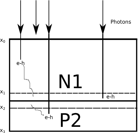
Most silicon photodetectors are based on a diode structure like the one shown in Figure 1. The crystalline structure of pure silicon is doped with different types of materials to produce silicon that uses holes (positive charges, and hence p-type) or electrons (negative charges, or n-type) as the majority carriers. When these two types of silicon are abutted, they create a diode, which only allows current flow in one direction. Furthermore, a region depleted of charge, called the depletion region, is formed at their junction. This is shown in the figure as the area in between x1 and x2. The width of this depletion region is a function of the relative dopings of the p and n silicon, as well as any reverse bias voltage placed between the n and p type.
When a photon hits the silicon, it penetrates based on the wavelength, and, if it is absorbed, will create an electron-hole pair where it absorbs. There are thus three places where this electron-hole pair can be formed, either in the p-type bulk, the n-type bulk, or the depletion region. If it is formed in the depletion region, then the electron-hole pair are swept away, thus creating a drift current, since current is created when charges move. If it is absorbed in the n-type region, the electron will remain, as the majority carriers in n-type are electrons, and thus the hole that is formed is left to diffuse toward the depletion region. This situation is reversed in the p-type silicon, where the electron diffuses. These diffusions also create a current. Thus, the total current in the photodiode is the addition of these two diffusion currents and the drift current, with the amount of current based on how many photons are hitting the sensor, as well as the sensor's area. A larger sensor can collect more photons, and can be more sensitive to lower light intensities.
To measure how much light hits the sensor, the current could be directly measured. The currents produced by the photoconversion are typically very small, however, on the order of femtoamperes (1e-15 A), which discourages an accurate direct measurement. Thus, nearly all sensors employ a technique called integration, where the voltage across the photodiode is set to a known potential, and the photodiode is then left to collect photons for a known period of time before the voltage is read out. Longer integration allows more charges to be converted, and thus measurable changes in the voltage can be detected.
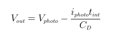
Equation 1 shows how direct integration works. Vout is the output voltage measured across the photodiode, iphoto is the photocurrent, which is assumed to be constant during the integration time, tint is the integration time, and CD is the capacitance of the photodiode. Since the capacitance of the photodiode is usually in the femtofarad range, this offsets the small photocurrent values, which are typically on the same scale, and so the change in voltage is magnified by the integration time into something that can be directly measured. Using a first order approximation, the capacitance and integration time are assumed constant, so the output voltage changes linearly with the amount of photocurrent, which is a direct measure of the number of photons hitting the sensor.
An alternate way to look at direct integration is to think about the capacitance that is present from the formation of the depletion region. When the photodiode is reset, the maximum amount of charge is placed on this capacitance. As photons are converted into charges, these charges are removed from the capacitor creating the photocurrent. At the end of integration, the number of charges left in the capacitor would be directly proportional to the number of photons that hit the sensor. If the number of charges could be measured, then the amount of light that hit the sensor could be as well.
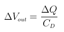
CCD sensors work by transferring the charge from one pixel to another until they end up at the periphery, and are then converted into a voltage to be read out. The charge transfer is accomplished by applying voltages that form wells of different potentials, so the charges transfer completely from one pixel to the next. Charges typically are shifted downward to the end of a column, then rightward to the end of a row, where the readout circuitry is present. The charge to voltage conversion then takes place, since voltage output is proportional to the charge over the capacitance, as seen in Equation 2
There are two main types of CCD architectures, frame transfer and interline transfer. In frame transfer, the charges from the pixels are moved from the photosensitive pixels to a non-photosensitive array of storage elements. They are then shifted from the storage elements to the periphery where they are converted and read out. In interline CCDs the non-photosensitive storage element is directly next to the photodiode in the pixel. The charges are then shifted from storage element to storage element until they reach then readout circuitry.
CCDs are designed to move charges from pixel to pixel until they reach amplifiers that are present in the dedicated readout area. CMOS image sensors integrate some amplifiers directly into the pixel. This allows for a parallel readout architecture, where each pixel can be addressed individually, or read out in parallel as a group. There are two main types of CMOS image sensor modes, current mode and voltage mode. Voltage mode sensors use a readout transistor present in the pixel that acts as a source follower. The photovoltage is present at the gate of the readout transistor, and the voltage read out is a linear function of the integrated photovoltage, to a first order approximation. Current mode image sensors use a linear relationship between the gate voltage of the readout transistor and the output current through the transistor to measure the photocurrent.
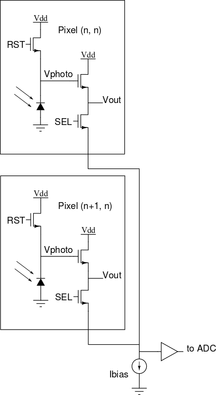
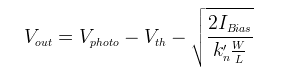
Figure 2 shows a typical three transistor voltage mode CMOS pixel [Nakamura2005]. The reset transistor allows the the photodiode to be reset to the known potential, the switch transistor allows the photo voltage to be placed on the readout bus, and the readout transistor converts the photo voltage to an output voltage that gets placed on the readout bus. The readout transistor is biased so that it is in saturation. The output voltage is shown in Equation 3. The voltage output follows the voltage input, minus an offset due to the threshold which is required to turn on the transistor, and an "on" voltage which is present because of the biasing current. K'n is a parameter of the process used to fabricate the transistor, defined by the mobility and oxide capacitance, and W/L is the aspect ratio, set by the pixel designer. The structure allows for a pipelined, column parallel readout, where the switch transistor will be activated one row at at time, and the voltage of the pixels is then readout from each column. The pixel is reset, and then then next row of pixels are read out, while all rows not undergoing readout continue integrating. The output voltage is then digitally sampled.
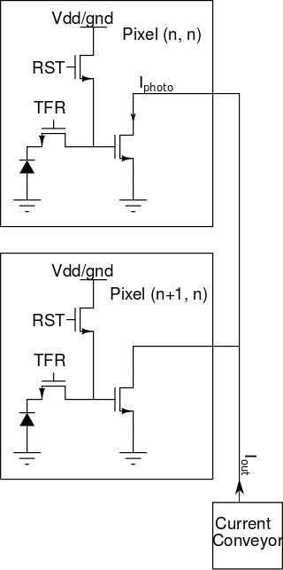
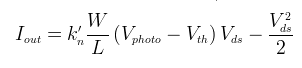
Figure 3 shows a typical current mode sensor, similar to the design presented in [Njuguna2010]. Equation 4 shows the current through a transistor in deep triode mode. The current is linearly proportional to the photovoltage, provided the drain to source potential of the readout transistor is kept constant. This is usually done with a current conveyor at the end of each readout bus, which mirrors the current while keeping a constant voltage on the bus line. The mirrored current can then be converted into a voltage and sampled. Alternate pixel architectures exist for both voltage and current mode imagers, the three transistor setup is the most typical.
When comparing image sensors, either CCD or CMOS, the system is essentially a box where the input is light, and the output is an image based on the light that is seen. The service provided by the sensor is the conversion of light to a digital image. There are a number of common metrics that are used for image sensors. These metrics will be explained below, as well as how they relate to the design of a sensor. These metrics can be used to facilitate an objective comparison of any type of image sensor, and most of them go beyond the notion of raw pixel counts. They will be grouped in three categories, metrics related to the pixel layout, metrics related to the pixel physics, and metrics related to the pixel readout. These categories are not hard and fast categories, as there will be some overlap amongst them.
The most common metric used in comparison of image sensors is the pixel count, usually expressed in megapixels, or millions-of-pixels, and it is regarded as a HB metric. The number of pixels in a sensor is a function of how large of a chip area the sensor designer has available. The designer must then know much of the chip can be dedicated to the pixels versus how much must be used for digital logic and readout circuitry. A key factor in this decision could be the number of devices used in a pixel. Being able to eliminate a device might mean the difference between a VGA format (640x480 pixels), and a megapixel (1000x1000 pixels). Another metric that goes hand in hand with pixel count is the pixel pitch, usually expressed in micrometers-squared or micron-by-micron. Since pixels are created in repeated arrays, the pitch defines how much area each pixel in an array occupies. Typically, the smaller the pitch, the more pixels that can be fit on the sensor. Smaller pixels, however, will not collect as much light, and thus may not be desirable for high frame rate imagers, or imagers designed for low light observation.
The pixel fill factor is another highly used metric that deals with how a pixel is physically laid out. The fill factor is listed as the percentage of the pixel area that is consumed by the actual photodiode, and is a HB metric. A fill factor of 100% would be ideal, as then all of the pixel area is used for photocollection. Some chips can achieve this by using a backside illuminated design, where the readout circuitry is placed below the photodiode, and thus it can occupy the entire pitch of the pixel [Suntharalingam2009]. Most sensors do not have a 100% fill factor, and a sensor designer has many considerations to make when deciding how much of the sensor to leave for the diode, and how much readout or charge transfer circuitry will occupy. Microlenses may be used to improve fill factor. Microlenses are lenses that are placed directly on top of the pixel, and they focus the incident light so that more hits the photosensitive portion of the pixel.
Some image sensor metrics are related to the physics of how photons are converted into charges. The discussion in Section 1 implied that all photons that hit silicon with the proper energy form electron-hole pairs as they are absorbed. This is not entirely true. Quantum Efficiency is measure of how many photons are converted into electrons-hole pairs, and is measured as a percentage. It is a function of wavelength, but usually the peak quantum efficiency over the visible spectrum is reported in data sheets. It is a HB metric, as ideally every photon would be converted into charge, regardless of wavelength.
The integrative method of gathering photocurrent is based on the capacitance of the photodiode. The capacitance, in turn, is based on the dopings, which are set by the process used in sensor manufacture, the pixel area, set during pixel layout, and the bias voltage, an operating parameter. The size of this capacitance creates a limit on the total amount of charge a pixel can hold during integration. This is referred to as the well capacity, measured in electrons. The well capacity leads to another important metric, the dynamic range, measured in decibels. The dynamic range is a metric of how well a sensor can measure an accurate signal at low light intensities all the way up until it reaches full well capacity. A HB metric, a higher dynamic range will allow the sensor to operate in more lighting conditions. Related to dynamic range is conversion gain which is measure as the change in output voltage with the absorption of one charge. It is proportional to the well size in most cases, as the output voltage is equal to the charge divided by the capacitance. A lower well capacity means a smaller capacitance, and thus a larger voltage change when a new charge is absorbed.
As new processes allow pixels to become smaller and smaller, a source of noise becomes more and more significant. This is dark current, measured in fA. Dark current comes from three sources; irregularities in the silicon lattice at the surface of the photodiode, currents that are generated as the result of the formation of a depletion region, and currents that are present because of diffusing charges in the bulk of silicon [Bogaart2009]. This current is added to the current from drift and diffusion in the photosensor, so that even if there is no current from external light, the pixel will still measure the dark current. Dark current is a LB metric, as the more dark current there is, the lower the dynamic range will be, since the dark current is robbing the capacitance of charge that can be used for photocurrent. Dark current is also a function of temperature, becoming worse as temperatures increase. It is typically listed on data sheets when measured at room temperature.
Due to process variations, the properties of transistors across the pixel array usually vary. The threshold voltages of readout transistors may not match, widths and lengths may not be exactly the same, the dopings of the silicon may have gradients, the mobility may also vary from pixel to pixel, and other nonuniformities will be present. These lead to fixed pattern noise, a LB metric that measures how much spatial non-uniformity is present in the sensor.
The reduction of unwanted noise is a very important aspect of image sensor design. Some of the noise could be inherent in the pixel, like shot noise, 1/f noise, and dark currents. Other noise can be present in the amplifiers that are used to convert the photovoltage into an output signal. The Signal-to-Noise ratio, measured in dB, is a ratio of how much of the original signal is present at the output, versus how much unwanted noise is present. It is a HB metric, as a higher SNR means more of the original signal is present at the output. Signal-to-Noise ratio usually varies by light intensity, as it is typically lower for dim light and higher for brighter light. Many sensor datasheets report only the peak Signal-to-Noise ratio. Percentage of linearity is another metric that is important, as it measures how linear the pixel output is with respect to the incident photovoltage. It is a HB metric, although 100% is the maximum linearly, meaning that the output is perfectly linear with the input.
The frame rate of an image sensor is the measure of how many times the full pixel array can be read in a second. Many sensors target ~24 frames-per-second or higher to be considered real-time. Power consumption is another important metric of image sensor design. Power consumption is a LB metric. The choice of supply voltage and pixel clocking frequency can have a large impact on power consumption, since power is measured as the product of the frequency, the capacitance, and the square of the supply voltage. Lower supply voltages mean lower power, at the cost of a decreased voltage range. Typically, the higher the frequency, the higher the frame rate, but at the cost of increased power.
The output bit-depth is another metric listed in many image sensor datasheets. Since the photodiode signal is eventually converted into a voltage, the bit-depth measures how much of a change in the output voltage can be reliably measured. Since the number of allowable output levels is 2bit-depth, the higher the bit-depth, the more distinct output levels there are, and thus it is a HB metric.
Since CCD sensors must move charge from pixel to pixel, the charge transfer efficiency is a metric that describes the percentage of charge that is transfered from CCD element to CCD element. It is a HB metric with a maximum value of 100%.
This section will look at a sample of the state-of-the-art in image sensors culled from the literature over the last five years. The dynamic range, dark current, and fixed pattern noise of CMOS vs CCD sensors will be presented using an analysis by unpaired observations. A model relating well capacity and charge conversion will also be presented. A discussion of the results will follow the analyses.
Here we will compare the performance of the dynamic range and dark current of CCD and CMOS sensors sampled both from the literature and from product offerings. The sensors are sampled from among the literature and product offerings. They are shown in Table 1 below.
Table 1: Stats for Sample Imagers
| [Manoury2008] | [Kodak2010] | [DALSA2009] | [Fife2008] | [CCD3041] | [Takahashi2007] | |
|---|---|---|---|---|---|---|
| Camera Type | CCD | CCD | CCD | CCD | CCD | CMOS |
| Well Capacity (in electrons) | 55000 | 40000 | 170000 | 3500 | 100000 | 14000 |
| Conversion Gain (in µV/electron) | 37 | 30 | 21 | 165 | 4 | 75 |
| Dynamic Range (in dB) | 74 | 68 | 82 | 57 | N/A | 69.9 |
| Dark Current (in pA/cm2) | 4 | 500 | 13 | 1008 | 14 | 1.5 |
| [Matsuo2009] | [Lee2009] | [Wakabayashi2010] | [Lim2010] | [Yasutomi2010] | [Suntharalingam2009] | [Moholt2008] |
|---|---|---|---|---|---|---|
| CMOS | CMOS | CMOS | CMOS | CMOS | CMOS | CMOS |
| 27000 | 130000 | 9130 | 4100 | 14000 | 130000 | 9000 |
| 45 | 105.4 | 75 | 110 | 38 | 16 | 162 |
| N/A | 97 | 71 | N/A | N/A | 51.3 | 72.6 |
| N/A | N/A | 17.7 | N/A | 34 | N/A | N/A |
Using analysis based on unpaired observations, the mean value of dynamic range for the chosen CCD sensors is 70.25 dB with a standard deviation of 10.532 dB. The mean value of the dynamic range for CMOS sensors is 72.36 dB, with a standard deviation of 16.268. The mean difference is -2.11 dB, and the standard deviation of the mean difference is 8.9811. The effective degrees of freedom are 8.48, so the t value for 9 degrees of freedom at 90% confidence is 1.833. The 90% confidence interval is (-18.572, 14.352), which includes a zero, therefore the CCD and CMOS sensors are not significantly different at 90% confidence when it comes to dynamic range.
Applying the same analysis technique to the dark current levels, the mean of the CCD dark currents is 370.8 pA/cm2, with a standard deviation of 445.18. The mean for CMOS dark currents is 17.73 pA/cm2, with a standard deviation of 16.25. The mean difference is 290 pA/cm2, and the standard deviation of the mean difference is 199.31. The effective degrees of freedom are 4.02, so a t-value of 2.132 is used. The 90% confidence interval is (-135.87, 715), which includes a zero, so neither is superior at 90% confidence.
There is a relationship between the well capacity and the conversion gain, as mentioned in Section 2.2. To further explore this relationship, a model of conversion gain based on well capacity is calculated using a regression. Because of the large range in values, the values are transformed using the natural log.
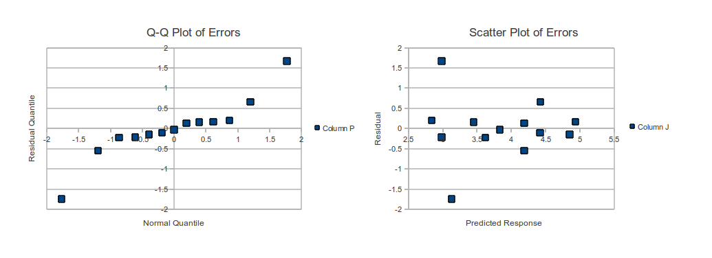
The results of the regression are as follows. There are 13 samples, so n is 11. The model is ln(Conversion Gain) = 9.3329 - 0.539*ln(Well Capacity). Doing an analysis of variance shows that the sum of squares of y was 204.2, the sum of the squares of the mean of y was 49.85, and so the sum of the total squares was 154.35. The sum of the squared errors was 6.807, and the sum of the squares due to regression was 147.55. Thus the coefficient of determination is 0.956, so the regression explains 95.6% of the error. The mean squared error is 0.618, and the standard deviation of the error is 0.977. The standard deviation of error for b0 is 2.159, while the standard error for b1 is 0.21. Using a t value with 11 degrees of freedom at 90% confidence, 1.796, the confidence intervals for b0 are (5.455, 13.211), and for b1 are (-0.916, -0.162). They are both significantly different from zero.
The results of the comparison based on the dynamic range and dark current show that neither the selected CCD or CMOS imagers are superior. This is expected based on the small sample size used for the comparison. Also, when comparing the dynamic range, the numbers are not much different for the CMOS and CCD imagers, which is reflected in the analysis. The means are fairly close for the imagers presented, differing by only 2dB. For the dark current analysis, the mean of the CMOS imagers is clearly smaller, however the wide variance of both the CCD and CMOS imagers does not allow for any conclusion to be said at a high level of confidence. Gathering more samples would help reduce the variance by a factor of 1/n1/2. A comparison based on other metrics like fixed pattern noise could also be done, but many sensors do not include this in their report, thus limiting the sample size.
The logarithmic regression of the well capacity and conversion gain shows that there is indeed a relationship between the two, as expected. Because of the negative slope of b1, the higher the well capacity, the lower the conversion gain will be. This makes intuitive sense, based on Equation 2. Looking at the quantile-quantile plot of the errors shows a mostly linear response, with the exception of two extremes. The same is shown in the scatter plot of the errors, which shows no discernible pattern, but also with a large error for the two extremes. The two extremes are the [Lee2009] imager and the [CCD3041] imager. The [Lee2009] imager was designed with an extra capacitance for overflow and active feedback, thus increasing the well capacity while still maintaining a high conversion gain. The [CCD3041] was designed for very low noise performance and not high conversion gain. Using the model can give insight into how large of a well a to use to achieve the desired conversion gain.
This paper described how modern image sensors work. It showed the difference in how CCD and CMOS image sensors function. It also gave a description of many of the common metrics used when comparing the performance of different image sensors. An analysis was performed using a sample of state of the art image sensors. The analysis showed that for dark current and dynamic range, no significant difference could be seen, although the sample size was small for both CCD and CMOS populations. A model was also developed that shows that a logarithmic relationship exists between the well capacity and conversion gain. The model predicts that smaller well capacities lead to large conversion gains, while larger capacities lead to smaller gains.
[Nakamura2005] J. Nakamura, ed., Image Sensors and Signal Processing for Digital Still Cameras. CRC Press, 2005.
A book which details much of the background on image sensors.
[Bogaart2009] E. Bogaart, et al. "Very Low Dark Current CCD Image Sensor," Electron Devices, IEEE Transactions on, vol. 56, no. 11, pp. 2496-2505, 2009. Available at http://ieeexplore.ieee.org/document/5247096/
A paper on a CCD designed for low dark current operation.
[Lee2009] W. Lee, et. al., "A 1.9 e- Random Noise CMOS Image Sensor With Active Feedback Operation in Each Pixel", Electron Devices, IEEE Transactions on, vol. 56, no. 11, pp. 2436-2445, Nov. 2009. Available at http://ieeexplore.ieee.org/document/5280321/
The paper describes a CMOS image sensor that uses active feedback capacitance to increase the dynamic range while reducing noise.
[CCD3041] Fairchild Imaging Corporation, CCD 3041 Back-Illuminated 2K x 2K Full Frame CCD Image Sensor, rev. B, 2005. Available at http://www.fairchildimaging.com/main/documents/CCD3041BIRevBDataSheet.pdf
This is a datasheet for a back illuminated CCD sensor from Fairchild imaging.
[Njuguna2010] R. Njuguna and V. Gruev, "Linear current mode image sensor with focal plane spatial image processing," in Cirucuits and Systems (ISCAS), Proceedings of 2010 IEEE Symposium on, pp. 4265-4268, June 2010. Available at http://ieeexplore.ieee.org/document/5537567/
The paper describes a current mode CMOS sensor that uses current scaling for processing.
[Manoury2008] E.-J.P. Manoury, et al., "A 36x48 mm2 48M-pixel CCD imager for professional DSC applications," in Electron Devices Meeting, 2008. IEDM 2008. IEEE International, pp. 1-4, 2008. Available at http://ieeexplore.ieee.org/document/4796668/
This describes a CCD image sensor from the DALSA corporation for large format cameras.
[Kodak2010] Eastman Kodak Company, Kodak KAI-2020 Image Sensor, revision 4.0 mtd/ps-0692, July 2010. Available at http://www.kodak.com/global/plugins/acrobat/en/business/ISS/datasheet/interline/KAI-2020LongSpec.pdf
This is the datasheet for a 2 megapixel Kodak CCD image sensor.
[DALSA2009] Dalsa Corporation, DALSA IA-DJ High Quanta Imaging Sensor, 03-036-200007-01, Sep 2009. Available at http://www.dalsa.com/public/sensors/datasheets/03-036-20007-01_IA-DJ-xxxxx-00-R_Sensor_DataSheet.pdf
This describes a CCD from DALSA that is designed for very high quantum efficiency.
[Fife2008] K. Fife, et al., "A multi-aperture image sensor with 0.7 µm pixels in 0.11 µm CMOS technology," Solid-State Circuits, IEEE Journal of, vol. 43, no. 12, pp. 2990-3005, 2008. Available at http://ieeexplore.ieee.org/document/4684639/
This paper describes a sensor that has very small pixel pitch.
[Takahashi2007] H. Takahashi, et. al., "A 1/2.7-in 2.96 MPixel CMOS Image Sensor With Double CDS Architecture for Full High-Definition Camcorders", Solid-State Circuits, IEEE Journal of, vol. 42, no. 12, pp. 2960-2967, 2007. Available at http://ieeexplore.ieee.org/document/4381466/
The paper describes a CMOS image sensor for camcorders that has low fixed pattern noise from doing double CDS.
[Matsuo2009] S. Matsuo, et. al., "8.9-Megapixel Video Image Sensor With 14-b Column Parallel SA-ADC", Electron Devices, IEEE Transactions on, vol. 56, no. 11, pp. 2380-2389, Nov. 2009. Available at http://ieeexplore.ieee.org/document/5280329/
This is a CMOS image sensor that is designed for very low fixed pattern noise.
[Wakabayashi2010] H. Wakabayashi, et. al., "A 1/2.3-inch 10.3Mpixel 50frame/s Back-Illuminated CMOS Image Sensor", in Solid-State Circuits Conference Digest of Technical Papers (ISSCC). 2010 IEEE International, pp. 410-411, 2010. Available at http://ieeexplore.ieee.org/document/5433963/
This describes a CMOS image sensor designed at Sony.
[Lim2010] Y. Lim, et. al., "A 1.1e- Temporal Noise 1/3.2-inch 8Mpixel CMOS Image Sensor using Pseudo-Multiple Sampling", in Solid-State Circuits Conference Digest of Technical Papers (ISSCC). 2010 IEEE International, pp. 396-397, 2010. Available at http://ieeexplore.ieee.org/document/5433971/
This describes a low noise CMOS sensor designed at Samsung.
[Yasutomi2010] K. Yasutomi, et. al., "A 2.7e- Temporal Noise 99.7% Shutter Efficiency 92dB Dynamic Range CMOS Image Sensor with Dual Global Shutter Pixels", in Solid-State Circuits Conference Digest of Technical Papers (ISSCC). 2010 IEEE International, pp. 398-399, 2010. Available at http://ieeexplore.ieee.org/document/5433976/
The paper describes a high dynamic range CMOS image sensor.
[Suntharalingam2009] V. Suntharalingam, et. al, "A 4-side tileable back illuminated 3D-integrated Mpixel CMOS image sensor", in Solid-State Circuits Conference Digest of Technical Papers (ISSCC). 2009 IEEE International, pp. 38-39,39a, 2009. Available at http://ieeexplore.ieee.org/document/4977296/
This paper describes a CMOS sensor that is back illuminated with readout circuitry present on a separate chip, integrated with 3D process technology.
[Moholt2008] J. Moholt, et. al., "A 2Mpixel 1/4-inch CMOS Image Sensor with Enhanced Pixel Architecture for Camera Phones and PC Cameras", in Solid-State Circuits Conference Digest of Technical Papers (ISSCC). 2008 IEEE International, pp. 58-59, 2008. Available at http://ieeexplore.ieee.org/document/4523055/
This paper describes a CMOS sensor designed for the Micron corporation.
| Acronym | Definition |
|---|---|
| CCD | Charge Coupled Device |
| CMOS | Complimentary Metal Oxide Semiconductor |
| VGA | Video Graphics Array |
| HB | Higher is Better |
| LB | Lower is Better |
| SNR | Signal-to-Noise Ratio |